Search photos...
Custom work
All
Photos
Illustrations
Designs
Collections
Contributors
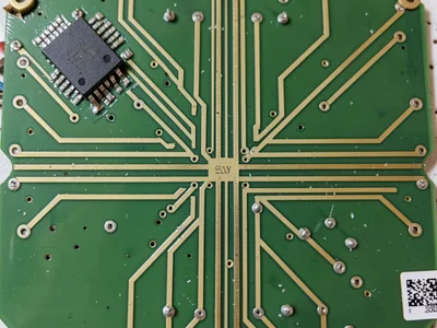
circuit
Orientation
Color
Exclude
Features
Sort by
technology
electronics
abstract
board
pcb
green
+4 more
chip
macro
silicon
pattern
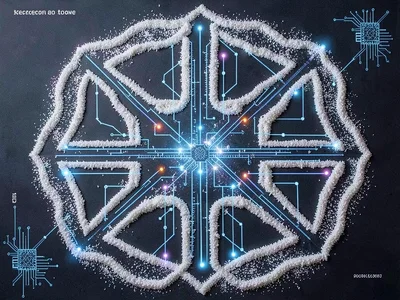
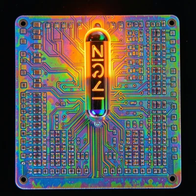
Petra Microworld
Download
Nan O'Gate
Download
Nan O'Gate
Download
Nan O'Gate
Download
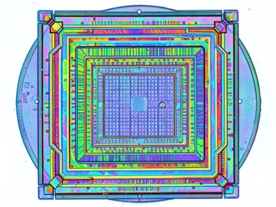
Prism Lahti
Download
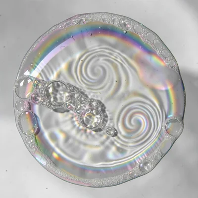
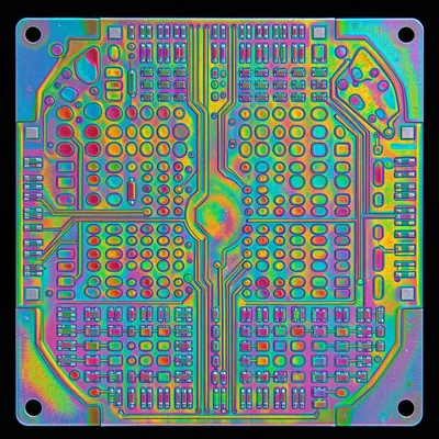
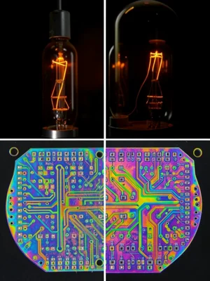
Resin Core
Download
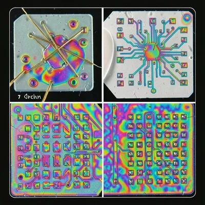
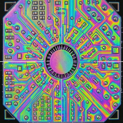
Kolam Circuit
Download
Nan O'Gate
Download
Nan O'Gate
Download
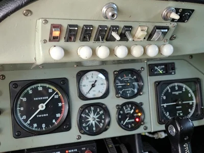
Altimeter Gyro
Download
Nan O'Gate
Download
Nan O'Gate
Download
Nan O'Gate
Download
Nan O'Gate
Download
Nan O'Gate
Download
Nan O'Gate
Download
Nan O'Gate
Download
Nan O'Gate
Download
Emma Blake
Download
Gradient Mach
Download
Tandem Verde
Download
Kolam Circuit
Download
Flatbed Fujiko
Download
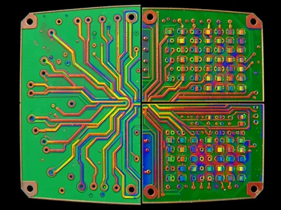
Trace Pathway
Download
Trace Pathway
Download
Trace Pathway
Download
Trace Pathway
Download
Trace Pathway
Download
Trace Pathway
Download
Trace Pathway
Download
Trace Pathway
Download
Trace Pathway
Download
Trace Pathway
Download
Trace Pathway
Download
Trace Pathway
Download
Nan O'Gate
Download
Nan O'Gate
Download
Nan O'Gate
Download
Nan O'Gate
Download
Nan O'Gate
Download
Nan O'Gate
Download
Nan O'Gate
Download
Nan O'Gate
Download
Nan O'Gate
Download
Nan O'Gate
Download
Nan O'Gate
Download
Nan O'Gate
Download
Nan O'Gate
Download
Nan O'Gate
Download
Nan O'Gate
Download
Nan O'Gate
Download
Nan O'Gate
Download
Nan O'Gate
Download
Nan O'Gate
Download
Phosphor Green
Download
Nyx Datacenter
Download
Resin Core
Download
Resin Core
Download
Resin Core
Download
Resin Core
Download
Resin Core
Download
Resin Core
Download
Resin Core
Download
Resin Core
Download
Resin Core
Download
Resin Core
Download
Resin Core
Download
Resin Core
Download
Devi Neon
Download
Tandem Verde
Download
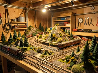
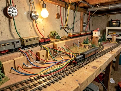
HO Scale Howard
Download
Skyler Nadir
Download
Nan O'Gate
Download
Nan O'Gate
Download
Nan O'Gate
Download
Nan O'Gate
Download
Umbra Meridian
Download
Petra Microworld
Nan O'Gate
Nan O'Gate
Nan O'Gate
Prism Lahti
Resin Core
Kolam Circuit
Nan O'Gate
Nan O'Gate
Altimeter Gyro
Nan O'Gate
Nan O'Gate
Nan O'Gate
Nan O'Gate
Nan O'Gate
Nan O'Gate
Nan O'Gate
Nan O'Gate
Emma Blake
Gradient Mach
Tandem Verde
Kolam Circuit
Flatbed Fujiko
Trace Pathway
Trace Pathway
Trace Pathway
Trace Pathway
Trace Pathway
Trace Pathway
Trace Pathway
Trace Pathway
Trace Pathway
Trace Pathway
Trace Pathway
Trace Pathway
Nan O'Gate
Nan O'Gate
Nan O'Gate
Nan O'Gate
Nan O'Gate
Nan O'Gate
Nan O'Gate
Nan O'Gate
Nan O'Gate
Nan O'Gate
Nan O'Gate
Nan O'Gate
Nan O'Gate
Nan O'Gate
Nan O'Gate
Nan O'Gate
Nan O'Gate
Nan O'Gate
Nan O'Gate
Phosphor Green
Nyx Datacenter
Resin Core
Resin Core
Resin Core
Resin Core
Resin Core
Resin Core
Resin Core
Resin Core
Resin Core
Resin Core
Resin Core
Resin Core
Devi Neon
Tandem Verde
HO Scale Howard
Skyler Nadir
Nan O'Gate
Nan O'Gate
Nan O'Gate
Nan O'Gate
Umbra Meridian
Refine with AI